Secure Elements are everywhere. They sit inside your smartphones, hardware wallets, e-Passports, payment cards, car keys, and SIM cards. They're tiny chips tasked with guarding some of the most sensitive data people carry. Most of them come with certifications and assurance levels that suggest near-invincibility. However, a growing body of research into fault injection attacks tells a more complicated story.
We spoke with Sergei Skorobogatov, a former member of the University of Cambridge's Security Group (founded by the late Ross Anderson), who has spent years probing the physical limits of these chips. He runs Cambridge Research and Engineering, which specializes in data recovery from damaged ICs and in analyzing semiconductor devices for backdoors.
We also interviewed Shivam Bhasin, a researcher based at the Nanyang Technological University in Singapore. Bhasin specializes in hardware security and fault injection; the art of using precisely targeted physical disturbances to make secure chips behave in ways their designers never intended.
What Secure Elements do
Before getting into how they break, we'll look into what Secure Elements are designed to resist.
A standard microcontroller, the kind found in a cheap IoT sensor or a basic Arduino board, stores its firmware and data in memory that can be read out with off-the-shelf tools. Connect a debug probe, and you can often dump the entire contents of the chip.
Some microcontrollers offer good protection, while others with better hardware security have backdoors in debug interfaces. Custom microcontrollers used in automobiles can resist many attacks due to a lack of documentation, a unique design, and the lack of blank samples. As a result, security levels vary across manufacturers and devices.
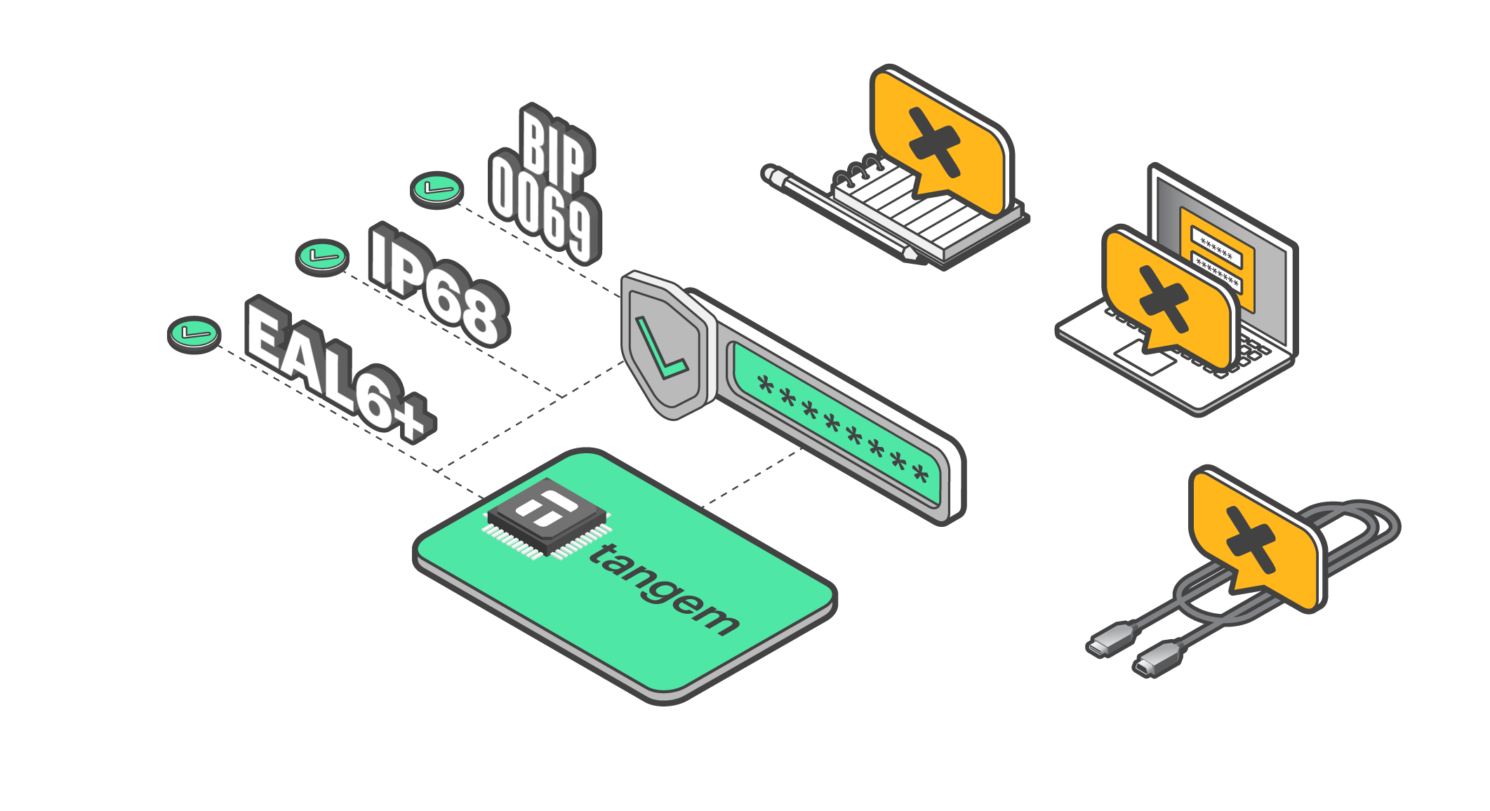
A Secure Element is designed from the ground up to resist both logical attacks (malicious software and protocol exploits) and physical attacks (probing, imaging, and tampering).
Its defenses include encrypted memory buses, active shield meshes that detect physical intrusion, randomized execution timing to frustrate side-channel analysis, and sensors that wipe sensitive data if the chip detects abnormal voltage, temperature, or light exposure.
Certification schemes like Common Criteria rank secure element chips on a scale from EAL1 to EAL7 based on the depth of their security evaluation.
Bhasin acknowledges the strength of this foundation. Secure Elements, he says, "are typically developed by established vendors with decades of specialized experience and undergo rigorous penetration testing and formal certification processes before deployment." But he adds a qualifier: "No system is entirely foolproof."
Why perfectly secure hardware doesn't exist
Skorobogatov is blunt about the limits of hardware security: "It is not possible to design a perfectly secure device," he says. "Any chip will inevitably carry flaws as a consequence of being designed by humans working from an incomplete understanding of every possible attack. Even specific hardware implementations, like Flash memory, can introduce vulnerabilities that weren't anticipated at the time of design".
Bhasin also emphasizes that security doesn't rest on any single mechanism.
"Modern chips rely on a chain of trust that starts with hardware as the root and systematically validates every component, from the secure bootloader to the verified application software," he explains. Each link in the chain checks the one above it. The hardware verifies the bootloader. The bootloader verifies the operating system or firmware. The firmware verifies the application. If every link holds, only authorized code runs on the chip.
The problem, Bhasin notes, is that "any manipulation of this chain can compromise the entire system, potentially allowing unauthorized or malicious applications to execute."
This is the foundation of fault injection. Attackers just need to find one link in the chain and disrupt it at the right moment. If the bootloader skips its signature check, it will load whatever firmware it's given. If a security flag is flipped from locked to unlocked, the chip's own protections stand down.
Historical examples
In 2010, researcher Christopher Tarnovsky famously defeated the Infineon SLE 66 CL PE, an EAL4+ certified chip used in Trusted Platform Modules and satellite TV cards, by combining chemical decapsulation, microprobing, and focused-ion-beam (FIB) circuit editing. Tarnovsky's attack required months of work and specialized equipment, but it demonstrated that physical countermeasures considered state-of-the-art at the time could be systematically defeated.
More recently, researchers have shown that even newer chips with more advanced shielding can be vulnerable to attacks that weren't anticipated during chip design. Flash memory, which Skorobogatov specifically mentions, has been a recurring weak point: its physical characteristics can leak information about the data it stores, and its write/erase mechanisms can be manipulated in ways chip designers didn't account for.
Structural issues at the fab
There's also a more structural issue baked into the manufacturing process itself. Most chips ship with test interfaces (JTAG ports, scan chains, proprietary debug modes) used for post-production verification and quality assurance. These interfaces provide deep access to the chip's internal state. They're supposed to be permanently disabled after factory initialization by blowing one-time-programmable (OTP) fuses or setting lock bits.
In practice, they represent a latent attack surface. "If an attacker finds a way to enable these features," Skorobogatov notes, "full access to the device could be reinstated." Researchers have demonstrated this across multiple chip families, sometimes using a laser to flip the specific bit that controls test-mode access, effectively "unblowing" a fuse at the logical level.
Reconnaissance first, lasers later
Attacking a Secure Element needs a structured methodology that unfolds in stages. Skorobogatov describes a process that typically begins long before anyone powers on a laser or connects a probe.
Stage 1: Information gathering
The first step is reconnaissance. Skorobogatov explains that most attacks begin with open-source intelligence: datasheets, developer documentation, patent filings, and even marketing materials. Anything that narrows the architecture. Attackers also study "similar devices with full documentation, or any predecessors with known vulnerabilities," working inward from what's already known to what isn't.
Researchers comb through publicly available datasheets, patent filings, developer documentation, academic papers, and even marketing materials. A product brief that mentions a specific processor core or memory architecture can significantly narrow the search space.
If a chip is a newer revision of a previously studied family, the attacker may already understand 80% of the architecture before touching the physical device.
Stage 2: Reverse engineering
The process moves into reverse engineering at multiple levels: support software, internal firmware, bootloaders, and eventually the silicon logic itself. The goal is to build a detailed operational map of the chip, revealing how data flows, where keys are stored, and which routines handle authentication.
Software-level reverse engineering might involve dumping and disassembling the firmware (if accessible), analyzing communication protocols between the chip and its host device, or studying publicly available SDK or driver code to infer the chip's internal operations.
In hardware-level reverse engineering, researchers chemically remove the chip's packaging to expose the silicon die, then image it layer by layer using optical or electron microscopy.
Specialized software tools can reconstruct the chip's logic gates from these images, eventually producing a schematic of the chip's internal circuitry. This process, sometimes called delayering, can reveal the locations of memory arrays, cryptographic coprocessors, random number generators, and security sensors designed to detect tampering.
Stage 3: Active attacks
With a map of the chip in hand, researchers move to active exploitation. The toolkit is broad: power analysis, electromagnetic and optical emission monitoring, laser fault injection, voltage glitching, and protocol-level data manipulation. Skorobogatov notes that each technique has its own trade-offs, but "altogether they give the result quicker and more efficiently." The real power lies in their combination.
Power analysis monitors the chip's electrical consumption in real time while it performs operations. Different instructions and different data values produce slightly different current draws, so a statistical analysis of many power traces can reveal secret keys.
Electromagnetic emission analysis works on a similar principle but captures the electromagnetic field radiated by the chip rather than its power consumption.
Optical emission analysis exploits the fact that transistors emit tiny amounts of infrared light when they switch. By imaging the backside of the chip with a sensitive near-infrared camera, researchers can observe which parts of the circuit are active during specific operations.
Power glitching involves briefly disrupting the chip's supply voltage at a carefully chosen moment during execution. If timed correctly, this can cause the processor to skip an instruction, corrupt a comparison result, or bypass a security check.
Protocol-level data manipulation targets the communication between the chip and its host. By modifying commands, replaying transactions, or injecting malformed data, attackers can sometimes trigger error states that leak information or bypass protections.
Laser Fault Injection (LFI): the precision tool
Among all these techniques, laser fault injection occupies a particular niche.
What sets laser fault injection apart, Skorobogatov explains, is its dual precision: it can target "a particular time and also a precise location within the device logic or memory." Where power glitching affects the entire chip at once, a focused laser beam can zero in on a single gate or memory cell. This gives the attacker two dimensions of control: when the fault occurs and where it lands on the chip.
Bhasin describes the degree of control LFI offers. "In a well-characterized system, a laser can target and manipulate specific bits with high accuracy.” The laser's bit-level precision "allows an attacker to target security flags that control the state of the system, effectively 'switching off' protections."
A security flag is a set of control bits that tells the chip whether it's in a locked or unlocked state, whether debug access is enabled or disabled, and whether the bootloader should enforce signature checks or skip them.
Fault that flag, and the chip's entire security posture can change, corrupting the output of a cryptographic operation and leaking information about the secret key. If a fault is precisely timed during a cryptographic operation, it can corrupt the output data and by analyzing these errors, an attacker can mathematically reconstruct and leak the secret key.
Economics of breaking secure chips
If Secure Elements can be broken, why aren't they being broken constantly? In the near term, the answer is cost.
Breaking into a Secure Element isn't a weekend project. The device typically has to be reverse-engineered at both the silicon and firmware levels before an attacker even knows where to look for an exploit. Skorobogatov puts the timeline bluntly: "This process could take months or even years to succeed."
Bhasin frames the cost landscape as a spectrum: “The equipment required for fault injection ranges from DIY tools costing a few dollars to state-of-the-art laser or ion-beam systems exceeding a million dollars”.
A basic voltage glitching setup can be built with an FPGA board, a MOSFET, and some creative soldering; total cost under $1000. A professional laser fault injection station runs $150,000 to $500,000. A focused ion beam system used for the most advanced circuit editing and analysis can cost over $1 million.
The track record bears this out. Skorobogatov notes that chips certified at EAL5 and even EAL6 have been successfully compromised, but only by "large teams of experts within specialized companies and government labs, and at great cost and enormous efforts".
Non-economic motivation
Bhasin points out that "non-monetary motivations, such as national security interests, legal requirements, or criminal forensics," can also justify the use of expensive and sophisticated attack vectors. A government lab analyzing a seized device isn't running a cost-benefit analysis in the commercial sense.
A large competitor with ample resources can acquire the same equipment, hire the same caliber of researchers, and invest time to break a rival’s secure element and weaken confidence in their product.
This dynamic already plays out in the hardware wallet industry. Ledger's in-house security lab, the Donjon, has published multiple rounds of research demonstrating successful fault injection attacks against Trezor devices, framed as responsible disclosure aimed at improving ecosystem-wide security.
What does this mean for holding crypto on hardware?
Physical attacks on individual consumer devices are generally not economically viable for most real-world threat models. But Skorobogatov warns against letting that fact breed complacency. Having a Secure Element inside a device, he says, "does not provide full assurance against any attacks." Given enough time and resources, a determined attacker can always find a way in.
The practical security of a hardware wallet depends on the full stack: the Secure Element, the firmware running on it, the communication protocol between the chip and the companion app, the supply chain integrity from factory to end user, and the choices the user makes.
One underappreciated layer of defense comes from how well-designed wallets handle key derivation. Many cryptographic devices don't store raw encryption keys directly on the chip. Instead, they store a hash of the user's password or PIN. The actual cryptographic key is derived from the user's input at the time of signing. This means that even total physical compromise of the chip doesn't hand the attacker the keys outright.
Even if an attacker achieves full physical access to the chip, Skorobogatov says, the payoff isn't guaranteed. If the user has chosen a strong password, all that's left is brute force (trying many passwords), and "that could take many years to succeed, even on very powerful servers."
The bigger picture
Cryptography provides mathematical guarantees. However, those guarantees live in physical hardware that operates in the real world, where transistors can glitch, photons can flip bits, and test modes can be re-enabled.
For chip and device manufacturers, this means security is an ongoing engineering discipline: monitoring the research landscape, updating threat models, and designing for resilience against emerging and sophisticated attack vectors.
For the end user, even though these methods are confined to high-resource environments, they serve as a reminder of the importance of physical custody.
While a fault-injection attack requires specialized equipment and significant expertise, it underscores that hardware security is about increasing the cost of an attack beyond the value of the assets protected.