Laser fault injection (LFI) is the most technically demanding attack in the hardware security researcher's toolkit. It involves firing a precisely focused infrared laser at the exposed silicon die of a chip to cause a specific transistor to malfunction at a specific moment during a specific operation. When it works, it can extract secret keys from chips designed to prevent such extraction.
Several publicly documented cases demonstrate that this technique has been successfully applied to dedicated secure chips used in hardware wallets and authentication tokens to protect cryptographic secrets.
This article takes a closer look at some specific cases. It also explains why laser fault injection isn't a significant concern for most hardware wallet users.
Laser fault injection proves that certified secure elements can be broken under laboratory conditions. It also proves that doing so requires six distinct operational barriers that cannot be removed, compressed, or automated.
What Laser Fault Injection Involves
Before we look at specific examples, let’s clearly understand what laser fault injection is and how it works.
The photoelectric effect
Semiconductor transistors are photosensitive. When photons from a laser source strike a transistor on a chip's silicon die, they generate electron-hole pairs, a phenomenon called the photoelectric effect at the semiconductor level.
A temporary injection of charge carriers can change a transistor's state. This means a transistor that should stay off can turn on briefly, or one that should hold its value can change. If this occurs at the correct transistor, at the right time, during the right instruction, it can cause the chip to work incorrectly in a controlled manner.
Transistors in modern security chips are measured in nanometers, so the laser spot must be focused to a few microns to target a specific functional region of the chip without triggering adjacent countermeasures. The timing must also be accurate to nanoseconds, and the laser energy must be calibrated to cause a controllable fault without permanently destroying the circuit.
What must researchers do before firing the laser?
Physical preparation of the device alone involves multiple steps, each of which can fail:
Component removal: The chip must be desoldered from the device's circuit board without damaging it. This requires hot air rework equipment and steady hands. A chip that is damaged during removal cannot be attacked.
Package decapping: The chip's plastic packaging must be removed to expose the silicon die. The standard method is chemical decapping with fuming nitric acid, a highly corrosive substance that requires fume hood equipment and chemical-handling training. The alternative is mechanical milling with a precision tool, which risks scratching the die. Either approach permanently alters the chip, leaving it without visible packaging.
Mounting: The exposed die must be mounted in a custom attack board that provides power, ground, and communications to the chip while leaving the die surface accessible to the laser. The board must be designed specifically for the target chip's pinout and power requirements.
Die mapping: Before any fault can be injected, the researcher must identify where on the die to aim the laser. This requires infrared microscopy to produce a photographic map of the die surface, combined with knowledge of the locations of specific functional blocks, such as the memory array, authentication logic, and AES engine. For a chip with no published die photograph, this mapping must be done entirely from the outside.
The parameter space problem
Even with the chip prepared and the die mapped, a laser fault injection attack requires finding the correct combination of three independent parameters:
The coordinates of the laser spot on the die (X and Y position),
The timing of the pulse relative to the chip's operation (measured in nanoseconds)
The laser energy (pulse duration and power).
Each of these has a wide range of possible values. To find the right combination that causes a useful fault rather than a crash, no effect, or permanent chip damage, we need to systematically explore.
The cases documented in this article required weeks of active parameter search before a successful fault injection was achieved.
What a successful LFI looks like and what failure costs
A successful fault injection produces any of the following controlled malfunctions;
A security check returns the wrong result,
A protected memory region becomes accessible
An authentication step is bypassed.
A failed injection produces one of three outcomes:
The chip continues normally (no effect),
The chip crashes and must be reset (losing any progress),
The chip is permanently damaged, and the attack must start over on a new specimen.
Permanent chip destruction during an attack is not unusual. In the Ledger Donjon work on the ATECC series, the researchers explicitly noted significant chip loss during parameter exploration. Each destroyed chip represents a failed attack attempt with no return and requires either a replacement chip from the same device or a new target device.
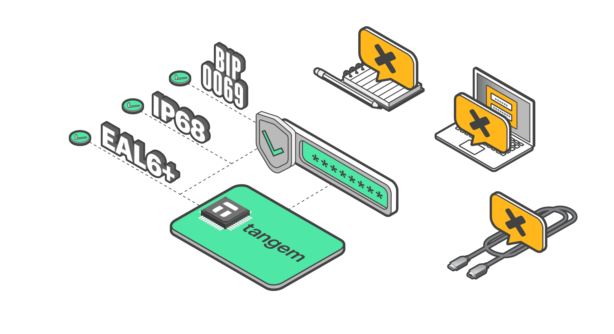
The ATAES132A is Microchip Technology's AES-based secure serial EEPROM; the first device in their CryptoAuthentication AES family.
The datasheet explicitly lists its physical security features:
Tamper detectors for voltage, temperature, frequency, and light;
An active metal shield over the circuitry; internal memory encryption;
Unspecified additional countermeasures.
It is not CC certified. Its security claims rest on the proprietary design described in its datasheet and on a ROM firmware that is not accessible for external review.
Research
Researchers from Fraunhofer AISEC: Bjoern Selmke, Endres Strieder, Johann Heyszl, Stefan Freud, and Thomas Damm, published their findings at FPS 2021 (Foundations and Practice of Security), with the full paper appearing in Springer's Lecture Notes in Computer Science series in 2022.
The project's main goal was to create a clear method for testing the security of chips that we cannot see inside, known as black-box laser fault injection. The ATAES132A chip was selected as a good example of devices used to keep information safe in real-world applications.
The attack methodology
The researchers had no access to the chip's source code, design documents, or photos of the chip itself. They started by using photoemission analysis, a method that captures the faint light emitted by transistors as they switch on and off.
By taking images of the chip during specific operations, they could see which areas were active during certain commands. This allowed them to create a functional map without needing to know the circuit layout.
Using this map, they identified candidate regions for fault injection, i.e., areas likely to contain the security-critical logic they wanted to disrupt. They then executed the parameter search: systematically varying laser position, timing, pulse duration, and energy across the identified regions while sending authentication commands to the chip.
The target was the chip's zone access control mechanism, which prevents unauthorized reads of protected user zones. The intent of the attack was to cause this check to return a positive result without the attacker having provided a valid authentication credential, allowing the contents of a protected zone to be read directly.
The attack succeeded. The researchers demonstrated full extraction of the secret key from a protected user zone via laser fault injection, without prior knowledge of the authentication credential.
Case 2: Microchip ATECC508A and ATECC608A
[ LASER FAULT INJECTION · Ledger Donjon · SSTIC 2020 / SSTIC 2021 · Black Hat USA 2020 ]
The Microchip ATECC508A is a secure element chip used across a wide range of IoT and embedded security applications, including the Coldcard Mk2 Bitcoin hardware wallet.
While it is designed to meet high security standards, including FIPS 186-3 and FIPS random number generator standards, the ATECC508A is not CC certified.
The ATECC508A attack in 2020
The target was the ATECC508A's data slot authentication mechanism. When the Coldcard Mk2 stores the seed, it is placed in a data slot configured as secret, readable only when authenticated. Authentication requires presenting the correct PIN hash. The idea here is that even if an attacker has physical access to the chip, they cannot read the slot without the PIN.
By firing the laser at a precisely identified region of the chip at the moment the access condition check was being executed, researchers caused the check to return a successful result regardless of whether authentication had been performed.
Physical preparation required: desoldering the ATECC508A from the wallet's PCB, milling away the chip's plastic package from the backside, and mounting it on an attack board. An infrared microscope was used to map the chip's layout and identify the target region.
Equipment cost: The laser fault-injection setup used by Ledger Donjon costs approximately $200,000, excluding the skilled technicians required to operate it and develop the attack.
The attack process is destructive; the chip's package is permanently removed, and it cannot be returned to service.
6 reasons why laser fault attacks don't scale
Six barriers prevent this laboratory attack from practically threatening hardware wallet users, regardless of the attacker's skill or budget.
Barrier
What LFI requires
Why does it prevent mass attack
Physical access
The chip must be desoldered, decapped, and mounted in a custom attack jig. The device is permanently altered.
Each target requires individual handling. An attack cannot be executed remotely.
Chip decapping
Chemical or mechanical removal of the chip's plastic packaging to expose the silicon die. Requires fuming nitric acid or precision milling equipment.
Irreversible. The device cannot be returned to service undetected.
It limits the attack to scenarios where device theft is already accepted.
Capital costs can’t be spread across multiple targets, as software can, in infrastructure.
Each chip also requires fresh parameter tuning.
Parameter search time
Identifying correct fault location, timing, laser energy, and pulse duration requires extensive. exploration of a large parameter space; days to weeks per chip family.
The time cost per target is high and largely irreducible. Prior research helps, but each chip variant requires fresh calibration.
Specialized expertise
Deep knowledge of semiconductor physics, fault injection theory, signal analysis, chip layout analysis, and embedded systems: a rare combination not available to hire off the shelf.
The pool of people capable of executing these attacks is small, known in the research community, and not available at a criminal-market scale.
Uncertain return
Success is probabilistic. Fault injection has a meaningful failure rate. The chips can be permanently destroyed without yielding the target data.
The expected return per attack attempt is discounted by the failure probability. Against average holdings, the math does not work.
All six barriers need to work together, multiplying their effect, rather than just adding up. This means an attacker has to overcome all of them simultaneously, making security much stronger.
The true purpose of laser fault injection research
Research that documents a successful attack against a chip actually makes them safer in two ways. First, it forces chip manufacturers to improve countermeasures in subsequent silicon revisions.
Second, published attack methodologies define the floor for what a well-resourced adversary can do and what chip designers must defend against.
Conclusions
Here's what you, as a hardware wallet user, should take away:
Laser fault injection is real, and it works. Researchers have cracked secure chips this way. In practice, it would require physically stealing your device first.
Once the attack starts, your device is visibly and permanently destroyed. You'd know it was tampered with.
The equipment costs a minimum of $100K–$200K. This isn't something a casual thief can pull off. It also takes weeks of skilled lab work per chip. It doesn't scale to attacking many people at once.
The attack can fail and destroy the chip with nothing to show for it, so it's a gamble even for the attacker.
If you're an average user, the economics simply don't work in an attacker's favor. Your real threat surface is phishing, malware, and seed phrase exposure, not a popular laser lab.